简介
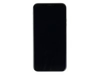
十年前,苹果推出了第一款iPhone并以此改变了世界。今天,我们拆解苹果的第十八次迭代——iPhone X。拥有圆润的边角和无边框设计,我们相信这是史蒂夫所设想的iPhone,但随着梦想的实现,这款新iPhone还会像第一款iPhone那样影响世界吗?时间会告诉我们,对于现在,我们的工作就是将其拆解并以此帮你判断。跟上我们的步伐吧,一起来看看苹果的宝石金冠如何闪耀。
感谢来自Circuitwise协助我们进行拆解工作,以及来自Creative Electron的X光图片,以及TechInsights帮助我们识别主板芯片。
我们有 澳大利亚店啦!
官方微信 iFixit中文站、
来跟进吧!
你所需要的
视频概述
-
-
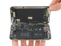
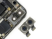
iPhone X已经到手!让我们来看看这个玻璃三明治里面有什么佐料吧:
-
A11仿生处理器(拥有神经网络)并嵌入M11运动协处理器
-
5.8英寸全面屏,OLED材质、支持多点触控的超级视网膜高清显示屏;分辨率2436X1125(458PPI)
-
后置双1200万像素摄像头,ƒ/1.8光圈广角镜头以及ƒ/2.4光圈长焦镜头,均配备光学防抖
-
前置ƒ/2.2光圈700万像素原深感摄像头,支持Face ID、1080P高清录像
-
支持快充技术以及Qi标准无线充电
-
我们这款A1865全球版基带芯片支持多个蜂窝网络频段,并支持802.11a/b/g/n/ac Wi‑Fi w/MIMO + Bluetooth 5.0 + NFC
-
-
-
iPhone已经走过了10年的漫长路途。事实上,iPhone的设计已经走过了一个轮回,这回的iPhone更像是我们最早的初代
-
和早前出厂的iPhone 8一样,iPhone X放弃了往年惯用的背面难看的环保标准标志以及型号
-
Jony终于拥有了他一直想要的无缝平滑背板。希望这些iPhone能不被回收商克扣地回收或是被粗鲁的丢进垃圾堆中
Here in Ireland (and I guess across the EU) we have the ‘Designed by Apple in California Assembled in China’ text, the CE mark and the ‘no dumping’ bin graphic still in place.
Tom Mooney - 回复
Anyone who thinks the markings on the back of the iPhone will influence whether it is recycled (rather than the trade-in value, accessibility of recycling facility or a customer’s own environmental awareness) has probably shoved a spudger too far up their nose.
Where did you get that minty fresh first-gen iPhone? Is it part of iFixit’s collection?
I’m really glad they took out the regulatory info on the back. It simply didn’t need to be there. You know you’re not supposed to throw an electronic away.
-
-
-
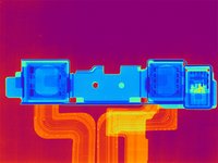
在我们开始毫无头绪的拆解前,先让我们看看来自Creative Electron为我们拍摄的X光照片吧
-
我们在其中找到了:
-
并非单独一块而是两块组合的电池,这是第一次在iPhone上见到这样的设计
-
一块超小的主板空间。看起来重叠的焊点似乎预示着有两层东西堆叠着。
-
为了给额外的前置传感器腾出空间,耳机听筒被下移了点
-
线性马达和底部扬声器之间有个神秘的芯片——我们很好奇它是什么
-
-
在这个步骤中使用的工具:iOpener$17.99
-
在这个步骤中使用的工具:Mako Driver Kit - 64 Precision Bits$39.95
-
像书一样的拆解步骤,这是让我们在iPhone 7 Plus上所惊讶的新设计,但现在已经成为了设计标准
-
单个挡板覆盖了逻辑板上的全部接口——我们从未如此高密度的接口布局
As mentioned above.
sean -
fixed i guess
My bracket only has 4 screws - the second from top (towards the right side of the phone) is missing - I bought the phone direct from Apple on launch day. Pretty surprised! Anyone else ever had missing parts?
-
-
-
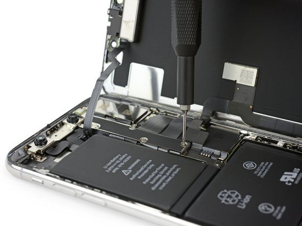
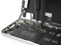
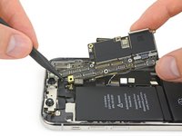
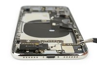
在卸下主板上各种挡板、接口后,我们终于可以看看这块最新的旗舰机的硬件了
-
稍后我们将更详细地分析下显示屏,现在我们利用X光看看这块神秘的芯片是不是被安装在了显示屏上
-
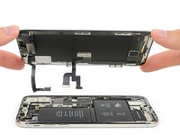
一个小的拆解步骤变化,当显示屏拆解后,前置摄像头将会被留在机身内
-
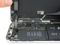
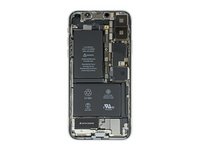
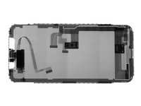
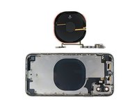
这张机身照片证实了X光照片中所看见的事实:大部分的空间都被这块双电池模组所占据,并且主板面积被大幅度缩小
-
-
-
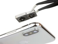
后置双摄有着一个坚固的支架,看起来这个支架将会对精密的组件提供一定的保护以避免出现“弯曲门”
-
双摄模组的另一面被用泡沫粘合剂固定在背板上,以防止因碰撞而造成的位移。这些摄像头需要人像模式或是类似的功能来展现他们的魔力
-
在背板上的玻璃罩周围你能看见密集的微小焊点,这是为了防止可能的相机与背板玻璃的碰撞
Might that beefy bracket be made of Liquidmetal (see https://en.wikipedia.org/wiki/Liquidmeta...)? That is, is it surpisingly stiff? Apple has an exclusive license to use Liquidmetal in consumer electronics, but seems not to have used it extensively.
-
-
-
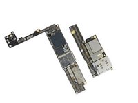
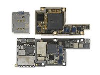
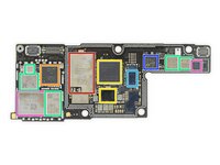
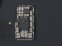
我们终于拆出了这个密集布置的主板,让我们好好地看看这块主板
-
这个小型化的主板非常节省空间,接口和焊件的密度是前所未见的,一克值千金,甚至Apple Watch的主板都有很多的空余处
-
紧凑的iPhone X主板装入了更多的高科技,这让身在其旁边的iPhone 8 Plus主板看起来是那么的粗糙与臃肿
-
比较两块主板的占地面积,iPhone X的主板大约是iPhone 8 Plus的70%——这让电池能够占有更大的空间
If that happens, how will users switch to other networks and install SIMs in their phone when they go abroad to avoid outrageous roaming charges?
-
-
-
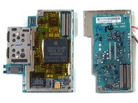
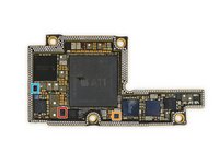
苹果是靠什么技术在原有面积70%的地方上加入更多的技术呢?那就是将一块主板对折
-
两块单独主板焊接在了一起,所以我们从我们的伙伴Circuitwise那儿借到了BGA工作台以分离两层主板
-
将两层主板分离后,我们计算了单个主板的面积并累加在一起,发现iPhone X的主板总面积是iPhone 8 Plus主板的135%,这就是苹果以退为进的办法
-
iPhone X的主板是我们从第一代iPhone以来看到的第一个双层主板(第三张照片)
You are missing the point. These are connecting the board physically, but there is no communication through those vias. You can see the other side of the board has all the connectors to flex. (On both boards). The third board act as a super stiffener to prevent overheating causing bending on the board. Great design!!!
Sorry Ramiro the outer row are shielding (ground) the 2rd & 3rd rows are comm lines between the boards (interposer board).
Dan -
Does the folded design take up more vertical space than the old logic board design, and if so, how did Apple account for this increased vertical space?
Was there vertical space open to begin with or does something in the design allow for more vertical space (i.e. the OLED panel is thinner)?
Thanks!
Yes, I think the OLED panel is considerably thinner. The X and 8 are pretty much the same thickness, so I think that that yes, it’s solely because of the OLED!
So Richard your assertion is that the silvered bumps all around the two boards are the vias? With a pitch of, what, 300µ?
The MacRumors article yesterday referred to an interposer between the two main boards, but I don’t see any such. Was MacRumors wrong, or am I missing something?
The outer perimeter of “silver bumps” aka solder balls is most likely all connected to ground. The rest must be signals. There is not enough cabling to support the required amount of signals between the two boards.
The interposer is still attached to the half in the top of the picture. The border of solder balls is higher than the rest of the PCB. This is required due to the night of the components on each PCB.
Truly incredible design. Passes data without cabling, affixes the two boards to each other without hardware, and creates an EMI shield without extra metal
Is that a piece of flat flex connected across two parts of the lower board? going right under the middle screw hole
It’s the ribbon from the camera’s which is poking up.
Dan -
Dan, I don't think so. Its completely sealed inside the sandwich
Thats just a kapton insulator sheet inside the sandwich. I thought you were talking about the other image.
Dan -
I believe it time to find some more of my good old LCD bonding 9703 3M anisotropic tape. That might be the ticket for servicing that motherboard. Still have some tape in stock, so my shop will service that motherboard, when parts become available.
Have a good weekend all.
Jan
How did apple manage to take out heat from their processor? I still couldn’t understand how is this working…
You are all wrong :-) look at the RF board, there isn’t a signle trace routed from the armada of solder-pads, so I’d say they’re purely mechanical & GND /tekhead
You do understand the PCB is made up of layers.
Their won’t necessary be any visible traces on the surface besides what space is there! It’s so packed the lines would need to be buried inside the layers. One of the functions of via’s is to bring signals up and down the layers, clearly Apple is leveraging this here through the interposer board.
Dan -
@kyle - Found a good image set from Tech Insights! Here’s the side views http://www.techinsights.com/uploadedImag... and http://www.techinsights.com/uploadedImag...
There’s a lot of need for intercommunication between the RF and the main CPU. There’s no other interconnect between the two boards. The perimeter vias have to be a communication bus.
Kyle Wiens - 回复
-
-
-
-
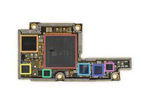
第一层主板:
-
苹果(Apple) APL1W72 A11仿生处理器,封装 海力士(SK hynix )H9HKNNNDBMAUUR 3 GB LPDDR4x 内存
-
苹果(Apple) 338S00341-B1 电源管理IC
-
德州仪器(Texas Instruments) 78AVZ81 充电管理IC
-
恩智浦半导体(NXP Semiconductor) 1612A1—可能是1610 Tristar IC的迭代产品
-
苹果(Apple) 338S00248 音频解码器
-
意法半导体(STMicroelectronics) STB600B0 电源管理芯片
-
苹果(Apple) 338S00306 电源管理IC
What are those “white stickers” in different shapes on the board? Are they the typical for checking water damage? Are the same shapes stickers related to each other in any way? Function?
Some of these components have a polarity. The white or black dot or a triangle denotes positive or anode end of the cap or diode.
Dan -
I think those are inductors, and the white spot indicates the right direction for them to go on the board.
Which is A11 Apple processor module part number, on same package row as SoC die designation APL1W72? The A11 Apple processor module part number has a format 339S004xx. The A11 photos are without sufficient contrast and difficult to read.
No help on A11 Apple processor module part number in this analysed iPhone?
Dimitar -
Is it me or are all the surface mount capacitors misaligned on the far right end? One is barely making contact with the pad. It’s like someone fudged it with their thumb picking it up.
Ian Melzer - 回复
I think that happens when you desolder it with hot air. It heats up the whole board.
which one of these chips are the thermal monitor? I have a damaged IPhone X that says the thermal monitor is dead.
I would be surprised if there is a separate chip for thermal monitoring. It’s more likely a function buried in one of the other ICs, probably one of the power management devices.
-
-
-
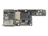
苹果(Apple)/村田(Murata) USI 170821 339S00397 WiFi/蓝牙模块
-
高通(Qualcomm)WTR5975 千兆LTE收发器
-
高通(Qualcomm)MDM9655 骁龙(Snapdragon) X16 LTE调制解调器和PMD9655 电源管理IC。但是苹果在调制解调器上采用了双供应商,TechInsights 在 A1901 型号里面发现了一个 Intel XMM7480 (PMB9969) 。尽管高通的调制解调器具有Gbit速度的能力,但苹果手机并不支持。
-
思佳讯(Skyworks) SKY78140-22功率放大器,SKY77366-17功率放大器,S770 6662,3760 5418 1736
-
博通(Broadcom) BCM59355 触控IC
-
恩智浦(NXP)80V18 PN80V NFC控制器模块
-
博通(Broadcom) AFEM-8072,MMMB功率放大器模块
Vic Lau, Qualcomm makes good chips at good prices, so there isn’t any reason Apple shouldn’t use them.
Yes, there is. They're suing each other.
If apple moves away from Qualcomm we can definitely expect a higher price tag on the next iteration of the iPhone
DAXimus -
The suing didn’t stop Qualcomm to get enough order apparently.
On the contrary,a higher price for customers to purchase iPhoneX seems to be the only result.
Theres more to it than the chips, It appears there are some licensing payments owed. Here’s a bit more Apple may completely drop Qualcomm as a modem supplier on future iPhone models
Dan -
Both those chips are present in Iphone 8 plus as well. They are just in different locations. Check step 10 in Iphone 8 plus tear-down.
Actually both the chips are required. MDM9655 is a baseband modem, and WTR5975 is a RF transceiver.
my Logic board has some damages to the circuit. I was thinking about buying another logic board (say iCloud locked) and transfer all if these chips. Will it work? Has anyone done it?
bijaya.pun - 回复
-
-
-
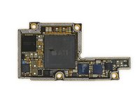
在这个三明治主板的外面:
-
东芝(Toshiba) TSB3234X68354TWNA1 64 GB 闪存
-
苹果(Apple) / Cirrus Logic 338S00296音频放大器
-
博世(Bosch Sensortec) BMP282 气压计
-
博世(Bosch Sensortec) 陀螺仪/加速器
Kapton tape on the underside for insulation, yeah
looks like the backside of the reader
anyone can tell that the storage its a TLC or MLC?
leartzajmi - 回复
And what to say about those two capacitors a bit off their solder points, almost touching the capacitor next to it ? Should’ve been failed in quality control, or visual inspection at least, no ?
Or …. Could it be the heat from you guys separating the boards, that made the components wiggle a bit and shift from their correct placement ?
The second one. ;) We’re doing this for the first time, often under less than ideal conditions, in a pretty big hurry. People who are more skilled and patient than I am can separate the boards and solder them back together flawlessly.
-
-
-
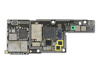
苹果做出了一个PCB三明治,但它是如何工作的呢?
-
A11仿生处理器位于主板的中央,你可以通过X光照片来进一步了解主板的3D构型,边缘环绕的圆柱体是用于连接两个主板的介质
Dan, most through-hole vias are hollow.
-> iFixit,
look again, there are no traces routed from those, so I don’t think any data is travelling through those. It’s just ground.
any relevant high-speed bus wouldn’t work well routed in that manner.
main board is the “computer“ where all the flexes come in to connect to screen & peripherals.
the rf-board is purely networking so very few wires has to connect between the main ARM and that board.
Albert, Review the comments in Step9 there is no other means for the two half to communicate with each other other than the vias and yes some are shielding (ground)
Dan -
Lel. Yeah. Those are just via stiching for shielding.
Maybe vias are security related. PCI homologation request for tamper-proof protection against encryption keys reading strait from RAM.
I think you are right! but I’m not sure that which chip to process security function.
-
-
-
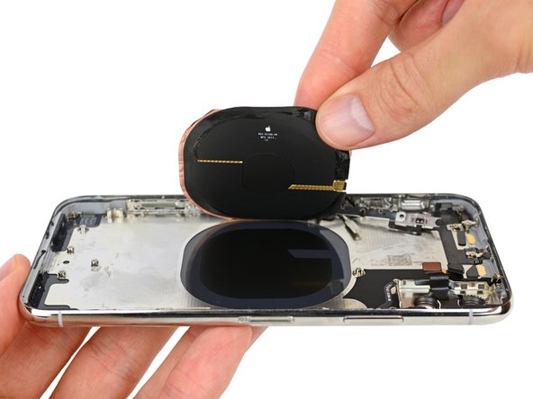
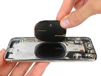
新的双电池模块带有四个电池拉带,类似于我们在iPhone 8系列中发现的较短的拉条,虽然它们朝向不同的方向
-
这块电池的能量为10.35Wh(2716mAh 3.81 V),仅比10.28Wh的iPhone 8 Plus电池大一点,但仍落后于12.71Wh的Galaxy Note8电池
-
双电池设计更多的是一种空间利用措施,而不是一个增加容量的措施, 两个电池的设计能让电池设计更具创意,以充分利用缩小主板后空余出的面积
It might be my age showing but what type of Li-Ion supports charging up to 4.35 ? (I mean .. there’s the type that goes up in flames but .. ?)
It is just a more stable battery that can handle higher voltage without damage. Even my Cubot Note S has 4,35V max voltage battery (4.150 mAh).
Okay so I use this phone for all the photos of appliances that we take at Jackson Appliance Repair Company. The question I have is— is the battery itself waterproof? Or is the phone waterproof (protecting components inside) when it’s fully assembled?
The device is waterproof. Batteries really can’t be made waterproof as they have exposed contacts which when shorted would be dangerous depending on how conductive the liquid was (i.e. salt water).
Dan -
-
-
-
你还记得Face ID技术吗?事实上我们在拆解工作开始前就已经尝试了它,我们的红外线摄像机帧数不足以拍摄下扫描时的点阵,但我们可以看见用于照明的灯光!
-
历史时间:过去,微软(Microsoft)做出了一个漂亮的空间定位传感器——Kinect。它采用了来自以色列的PrimeSense的红外点阵技术
-
苹果在2013年花费了3.6亿美元收购了PrimeSense,并且在之后的推向市场过程中投入了数亿美元
-
与此同时,微软陷入了困境之中,其不得不开发出一个新的传感系统用于Kinect 2。而现在iPhone有了深感传感器,说不定有人会把它装在无人机上!
@kyle tell your design team to add a play button over the image, people can easily miss that it’s a video. I thought it was just an image, but saw the comment about he enjoyed watching the video - so i hovered my mouse and then that’s I figured it’s really a video. :)
It’s IR. Human eyes can’t see it, so unlocking with Face ID is essentially just staring at it, and from the user’s perspective, it magically unlocks. No visible flashing here!
Jody, the flashes are invisible to the human eye. In the video you can hear the guy with the phone asking if the cameraman can see the flashes, because you need a special camera to view them. It’d be like staring into the end of a TV remote control and pushing buttons.
Not for me. I can see infrared easily.
Esa luz que nosotros no vemos, sera dañina de tanto uso ?. Porque desbloqueamos el telefono muchisimas veces al dia.
That light that we do not see, will be harmful of so much use? Because we unlock the phone many times a day.
Here’s a good vid on the FaceID projector lighting up someones face: https://youtu.be/OvVKnC6gGtg Jump to 5:50 to see it.
so why MS did not buy ++PrimeSense?++
Having designed a lens system for Occipital’s Structure sensor (which is also a Prime Sense derivative). The structured light emitter, which is actually a laser; vibrates to create the pattern that bathes your face. I am pretty sure the structure light source does not have the power to do anything besides scan your face, but also the infrared camera is lens system is probably tuned for 300 mm-500 mm unlike the Kinect(1), ASUS XTION or PrimeSense’s own early versions, which have a much longer range. If anyone is interested in doing more than just face scanning, check out Occipital’s website.: https://structure.io/ .
i wonder who makes the sensor subassembly - that must be a very intricate design; tying the processing and interface to the VCSELs that generate the light powering the activity
-
-
Surely the ir camera senses the ir flood projector, not the standard camera…
There are three IR light sources used: The small pencil beam to see if the phone is face down or next to ones face (proximity) which uses the camera as the sensor (located just to the left of the speaker slot from the front). Then there is the flood illuminator which lets the camera ‘see’ if you are there (to discriminate there is a face present) just to the right of the camera. The third is the dot projector (on the right side of the speaker slot) to ID you. The same camera is used for all three functions no special IR camera here.
Can I buy that TrueDepth system?
JJ Delisle - 回复
Has anybody figured out, if this part is replaceable? I hope this isn’t handled like the TouchID which is locked to the logic board?
-
-
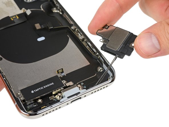
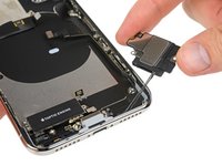
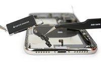
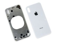
拆解即将完成,我们现在将会开始背板的拆解
-
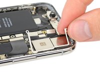
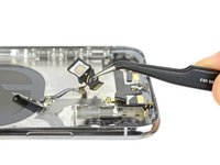
第一个取出来的是一个带有弹簧连接器以及EMI接地触点的小支架,并带有一条带状电缆
-
接下来是低音喇叭模块,在其接口周围充满了用于防水的粘性防水胶
-
最后,我们拆出了Taptic Engine和著名的气压计, 苹果的Taptic Engine仍然是一个线性振动电机
Are there two speakers at the bottom?
Nope just the one lower speaker. The second speaker is mounted to the upper portion of the display assembly.
How is vibration motor installe, it is glued or screwed?
A: Screwed. ;)
Do you sell replacements of the little bracket that is covered in spring connectors and EMI grounding fingers, and has a ribbon cable stuck to the back? As I was removing my screen to prepare for a replacement I saw that it had some damage. I don’t want to purchase a replace screen and find that it won’t work because of the damage to this part.
Caleb for some strange reason iFixit do not sell the EMI Grounding Finger plate nor do they sell the wifi flex cable that is attached to the underside of that plate. I had to go to Amazon to source a replacement for both. I think they should also stress how delicate those grounding fingers are, they are like tissue paper and can be damaged very easily if touched so take extreme caution when removing and reinstalling the plate and the attached flex cable.
Do you have links?? I can not find it.
Nice and informative post very helpful thanks for it, MS OFFICE 2019 MAC with lifetime license 70% Off.
Does anyone know the purpose of this bracket "covered in spring connectors and EMI grounding fingers"? What would be the possible side effects if it was damaged?
-
-
-
一如既往,我们的拆解工程师完美地使用双镊技术移除了Lightning接口
-
对于任何想拆除充电底座的人的好消息 lighting连接器看起来更加坚固,有更加宽的基板
-
正如我们之前所猜测的,它还带有用于之前我们所见到的插销式梅花螺丝穿过的小孔,使螺丝得以穿过并插入显示屏插销中
I don’t think it really matters. Apple’s Lightning Connector is double sided, so EVEN IF they DO have contact points on both sides, they probably would have wired them together anyway.
The Lightning connector IS double sided, however the pins are NOT NECESSARILY physically tied together in the connector; ergo it actually supports 16-pins, not 8. So it DOES matter. A double-sided port could hypothetically support Thunderbolt, or 2 USB3 channels. And we have seen, inexplicably, a double-sided port from Apple before in the iPad Pro. A fully 2-sided Lightning connector/port could be functionally as capable as USB Type-C, minus the legacy USB 2.0 lanes. (The Type-C connector ALWAYS maintains a legacy USB 2.0 pair; Apple would have no need for that legacy combination if Thunderbolt was their forward-looking target.)
Scott,
Apple has already defined the connector https://en.wikipedia.org/wiki/Lightning_... I doubt they are going to mess it up making it polarized directionally at this point.
Dan -
There are 2 separate parts here. One is the Lightning connector and the flex cable under it is the loud speaker flex cable.
-
-
-
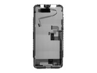
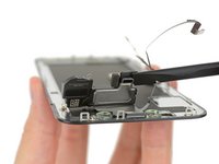
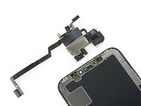
随着主要部件被拆解成零件,我们将注意力转回显示屏。我们注意到了听筒,苹果重新设计了一个新的声道,以便导出声音
-
小心地拆除显示屏上方的组件,我们看到这是一个我们从未见到过的最复杂的组件,在这上面集成了扬声器、麦克风、环境光感应器、泛光照明器以及距离传感器
-
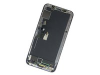
拆解掉全部组件后,我们只剩下了一个空的显示屏
So what was that mystery chip first shown in the x-ray pictures?
Where can I find a replacement upper display? Accidentally tore my wire ribbon slightly…
-
-
-
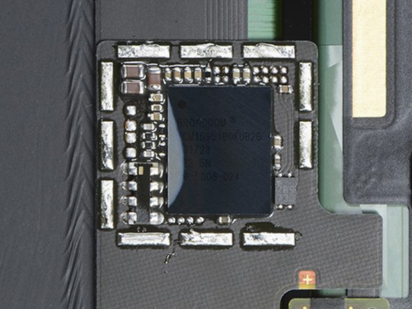
来看看内部神秘的芯片吧!在我们朋友 TechInsights 的帮助下,我们得以一窥屏幕盖子内部,我们有了以下发现:
-
标记为 BCM15951B0KUB2G 的触控屏控制器。
-
同时:我们从未见过的一个新的 STMicro设备,一个OLED电源管理IC,标记为 10 THADT733 X-139U。
The ST is more likely a boost converter, look at the inductors around it.
Too few pins to be a oled display-driver
-
-
-
回到已经被拆解差不多的iPhone X中框,我们见到了另一个熟悉的部件——这个密集的线圈:无线充电线圈
-
上面携带了大量的组件,包括音量按键、响铃/静音开关以及一个不知名的传感器支架
-
我们在顶部也拆除了一条很疯狂的多功能电缆,其集成了4-LED原彩闪光灯以及电源按键,就像是昔日的iPhone一样
Is the Qi coil that needs to be unobstructed for wireless charging just the center circle the ribbons are attached to or is it the whole unit?
You can see the coil in step 3 x-ray images.
Just the big black coil.
Is there anything special with the charging coil? Do you think they are being modest and when airpower comes out it will blow away qi coils?
-
-
在这个步骤中使用的工具:Jimmy$7.95
Could you show the other side of the stainless shell? Is the glass apple logo and lettering at the bottom printed on the backside and glass layer over top?
Yup, same as the 8, you can see the bare inside of the glass here.
looking for this solution
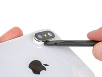
How was the camera bump removed?
Ivan Beatz - 回复
Destructively. It’s welded into place from the inside.
I find using a small flat head at each one of the weld points and rocking it left and right with a little force helps break the weld with less trouble than trying something large like a jimmy tool.
I opened the phone, removed the rear cameras, flash, logic board and battery, then wedged something underneath the rear camera bracket (which is spot welded to the camera bump) to break the spot welds to the camera bump. You’ll end up destroying the bracket (my replacement glass came with a new bracket and camera bump/lens) the bump will literally fall out once done. The rear glass can then be removed and replaced, then fit new camera bracket (and camera bump if damaged when removed).
Feel like doing a walk-through on this with photos for those less-inclined to break their new iPhone just because of a smashed back panel? :D
Absolute joke. After having spent all day painstakingly removing every single glass shard from the rear I find out that the bloody rear replacement glass doesn’t fit over the camera bump anyway…
Is there not a version that just fits over the bump even if it leaves a tiny gap ??? There is no way people will want their cameras/mics butchered. Failing that, it seems a bit excessive to strip down the entire phone just to remove a welded bracket. Frankly it is RIDICULOUS and I have been doing smartphone/tablet repairs from day 1.
It’s my own fault for not researching the subject. I wrongly assumed it was like previous models where it’s just held in place with adhesive tape.
This same kind of thing happened to me when the iPad airs came out and I thought it was still possible to do ‘glass only’. I think the only way I will learn is from not doing Apple repairs anymore!
Anyway well done Apple for catching me out yet again…..
Further update… Managed to find a seller on eBay who sells the rear glass covers with a slightly larger camera hole so it fits straight over the bump/lens. While this isn’t a perfect solution as there will be a bit of a gap it does makes it a million times easier and actually becomes feasible to do this repair (if you don’t mind hacking away at glass all day!).
My initial outburst was mainly because I was doing this job as a gesture of good will for someone and just assumed it to be straight forward. If it was my own phone or that of a close family/friend I would have just stripped it all down and done a proper job.
Hope this helps someone!
I use glass from aliexpress with normal hole with separate camera holder. If you put big hole glass you have the water resist problem.
Zeljko -
-
-
我们希望你们能喜欢我们这套带有22道菜点的菜肴,我们觉得他们应该很有营养
-
如果你错过了iPhone 8或是iPhone 8 Plus的拆解,你可以借此进行一些比较,并随时查看我们的可维修性分数
-
再一次感谢此次拆解的助力者们,Circuitwise、Creative Electron以及TechInsights!
-


146条评论
Incredible and dense tech inside this iPhone - thanks ifixit!
Wow! So exciting!
Hello,
Could you give us more info about NFC antenna localization? I suppose it’s on top of the back panel (to avoid conflict with Qi )
Thanks
It’s the top bezel itself, as always.
Tom Chai -
From Iphone 6 to XS Max, its always been on top?
Exactly! Given the amount of effort they put into shrinking (or folding) certain parts, it’s great to see they’ve put in the same effort to not make it harder to repair. That any modern smartphone will never receive a 10/10 score due to the design choices is acceptable, so I’m happy to see there’s still a reasonable way in. Not like some tablet/laptop hybrids that are horrendous to even open up; yes I’m looking at you Microsoft!
is the face id hardware programmed to the phone like the touch ID was? that would make replacing it impossible by 3rd parties.
i know its not connected to the screen, but still it may be a common repair like it is now.
There isn’t really a reason why replacing the True Depth sensors should be a “common replacement” like the home button was. The home button had to be replaced because it was a physical piece of hardware that was pressed millions of times before failing. The True Depth sensor should fail rarely since it is protected under glass and won’t be hammered on constantly.
Very good! Finally different in the interior, the previous models were all the same!
Question which iPhone X version is this? with 2 Qualcom chips it looks like it is the Model A1865
We analyzed the A1865. TechInsights opened up an A1901.
Apple claims that in order to make the screen curve with the edges, they had to fold part of the OLED screen over to hide the display driver right under the screen. Would you be able to verify that?
yes, there was an animation in the promo video. Looked weird. I’d like to know how they get the cutout in there.
And how do the cutout pixels account to the display resolution?
Andi -
Yes I saw this too, can you investigate more into the OLED display? In the video at 0:30, Jony Ive says “the custom OLED panel was engineered to fold and seamlessly combine with the external surfaces.” Their computer rendering really makes it appear there are hundreds of hidden pixels being illuminated. https://youtu.be/K4wEI5zhHB0?t=30s
Sweet! I’m actually impressed by the efficiency of this.
The picture of the sandwich board is tilted and out of focus. Please retake from directly above
Hey Mitch! We have top down photos of the logic board in steps 9, 10, 11, and 12! Check them out! The photo in step 13 is meant to describe depth, so the angle the focus on the chips inside is intentional!
Please post XRay Wallpaper of the iPhone X! You guys are the only ones that do it right!
Just snag the xray ‘wallpaper’ off the enlarged picture above… o.O
From a boardlevel repair perspective I sense this is mostly game over.
Separation of the two layers requires an amount of heat applied to the whole structure pretty much all soldering folks would consider unsafe including myself.
Lets all hope very strong that this design improves mechanical stability to a point where we wont have breaking solder joints any more and improved circuitry preventing most common damages. The level and style of catch up game with the repair industry apple plays here is disconcerting.
After settling with recent macs not to be considered buyable because of &&^&^$^ all components being soldered in and tethered added to ridiculous toylike features driving stupid prices now the iPhone is also beyond what I am willing to accept for such money.
Its depressing to see how fast apple from year to year is becoming more about profit and money and less about tech and users.
I wonder how long I have to wait until some other player comes up with a real alternative in terms of user experience.
Yes i agree, what they did will make repairs harder you can see in this pictures some components moved from their place after separation which is a bad outcome.
Have you considered the Essential Phone? It seems like they may have something special over there…
Gino J -
I have to agree. I started out in 1980 with my bsee degree repairing Apple 1’s 2’s and 3’s with an oscilloscope, soldering iron and the latest copy of the ic circuit handbook. I have not been thrilled about Apples progression from everyman’s or women’s mac to unserviceable sometimes throw away stuff that needs cottage industries to support what they can, when before it was mainstream repair with dig this, a service door!.
@Ross Elkins: The Apple 1, ][ and /// were designs based on 7400-series TTL logic. Do you have any idea how big, power-hungry (and expensive!) devices like the iPhone would be, if they were designed with 7400 chips? If it would even be possible (which I seriously doubt), the PCBs stuffed-full of TTL logic would easily cover a football field, would require a 1000A power supply, and would cost $100,000 (or more)!!!
For you to even mention the repairability of stone knives and bearskins designs (no offense meant to Mssrs. Wozniak and company) like the first few Apple computers in the same breath as state of the art, massively-integrated product designs like the iPhone X strongly suggests that you wasted your money on that EE degree; because you certainly haven’t been keeping up with technology, even at a lay,an’s level.
Yes, serviceability has definitely lost ground to compact design over the years. There are trade offs everywhere and either we carry around a brick with a removable back panel for component repair/replacement access, or have the smartphone design we do today where it's practically an extension of our body. I'm for the latter.
I do love iFixit teardowns though, daring to go where no one is intended to.
I salute you, iFixit!
gamma
@atomicsymphonic Umm… you have to FREEZE it to get it open! Essential Phone 拆解 It got a repairability score of 1.
Does the bottom left of the phone still just have a dummy panel covering the speaker grill?
If you’re thinking of the barometric vent, then yes! You can see it in the third image on step 17.
It looks like the mysterious chip was attached to the lower speaker…any idea what it is used for?
It is still mysterious!
Does the mystery chip possibly contain the data for the user’s facial recognition? Apple said that data would be stored on the phone only - and nowhere else - out of privacy concerns.
HL Dash -
Were you able to verify that face recognition still worked once the phone was re-assembled?
Cindy Leek - 回复
Facial Recognition works. But proximity sensor has to be swapped over to maintain Face ID after a screen swap.
iv tried today to swap screens on two iPhone X without swapping over any parts, just the screens and Face ID stopped working on both. ill try later to swap the proximity sensor to see if that fixes the Face ID.
roy -
I swapped two screens from one to the other on the iPhone X and Face ID stopped working on both. ill try later to see if swapping the proximity sensor fixes the Face ID not working.
roy -
Should be much easier to repair without the virtual touch id button.
John Knirr - 回复
this looks like a science fiction movie, very big WOW
Be nice if the person breaking down the phone, or at least the one who writes up the Teardown, had some engineering training, some of the text above was completely unintelligible, unscientific and used wrong terminology in descriptions. Apart from that, though, great! LOL
And you’re perfect in everything that you do right? If you’re so smart you should have filtered through all type O’s and kept your rude post to yourself, JACKASS!!
Stay tuned ;)
The next thing to go is the nano sim tray for sure it's so large compared to the logic board.
Apple’s almost definitely going to replace it with an eSIM in the next model. I sure hope so. https://www.blog.google/products/project...
What about the screen essentially folding backwards on top of itself? I was wondering about that in a tear down like this. Here’s what I’m referring to: https://boygeniusreport.files.wordpress....
We picked up an A1865 in Australia!
Maybe I missed it, but did we find out what the chip next to the speaker is? It was called out with a green box on the X-Ray in the 3rd step. I don’t think i saw the explanation.
gregkramer - 回复
I believe you’re talking about the chip in Step 20!
Just a guess, but the “Unidentified sensor bracket” in Step 21 could be related to Apple’s new leather folio case which wakes the phone upon opening and sleeps upon closing.
I’m sure the IR proximity is what does that
Dan -
It’s unlikely to be the proximity sensor doing this, as then it would work with third party cases as well, not just Apple’s and would do something similar when just covering or uncovering the screen.
In the iPhone X promo video from Apple, we can see the OLED screen is curved under itself, which I’ve read is to ensure a consistent light all the way to the edges of the phone.
_
I’ve looked above a few times at the various steps but don’t seem to find any reference to details on the OLED screen, which you’d imagine is a very important part of any smartphone.
_
iFixit, can you please add a 24th step that goes into detail on this? I can see from a couple of comments above that I’m not the only person wanting to know.
_
Thank you for your incredible work!
_
Regards
_
Alex
Any idea who they are using for the Qi charging IC?
Apple made there own coil. It has the apple insignia on it
zachary -
Are you able to put the phone back together and have it still be functional, or does this tear-down destroy the phone?
The degree of consolidation for functionality in the circuitry is unprecedented! State of the art.
Very nice, good explain
Very informative! I love your site!
Ram wasn’t mentioned this year? What is it? How much ram?
3 GB of RAM in the A11 chip
Dan -
Face id only works if the phone is vertical.
John Knirr - 回复
Any commentary on the antenna design and how it compares to 8/7 (plus/nonplus)?
iPhone X is the same wireless charging hardware design like iPhone 8 ? any difference?
Excellent site do you only describe etc phones?
IFIXIT covers many different products review the other tear downs here: https://www.ifixit.com/Teardown
Dan -
I just hope no costumer comes in with a broken rear…
thanks lot for all ifixit team
So amazing PCBs layout!
Would appreciate your comments about the Snapdragon X16 Modem. Have the aireals been disabled by Apple in a smilar fashion to the way they were disabled on the Iphone 8 and 8Plus model 1865? This seems to be an important issue? Jack
This is too cool ! Do you have data on which parts are best in class the industry offers ?
lol Apple REVEALED! KUDOS IFIXIT
Hi, I know that the iPhone X supports the auto sleep/wake function, as on iPads, using wallet covers like the original Apple Folio one, so I think there should be magnets inside the phone, is that true? If yes where they are? I saw tons of wallet covers on eBay that are sold as "magnetic" but they don't say if they support the auto sleep/wake function, anybody has tried one of these? Thanks
Fantastic teardown guys!! I am curious about the stainless steel ring around the frame. It does appear that it’s composed of 4 distinct pieces due to the seams between.
Can you guys comment on how they’re connected to each other as well as the backplane?
It does make me wonder on the Space Grey version - are the 4 pieces PVD coated before they’re joined or after?
I work for a phone company and we are getting these phones returned by same group of people, they take the phone out then 24 hours they return it, the boxes are open but the phones are still in the plastic seals, it there anything that can be done to these phones they look as good as new but my gut is saying something has been done with the phones.
Hello, please, iPhone X has two or only one bottom microphone? On picture is only one, and iPhone 6S, 7 have two.
How the on screen finger print works? what kind of part’s it need to execute?
There is no in screen touch ID. Just Face ID, and there’s no fingerprint reader anywhere on the phone.
Hi, please, where is fourth microphone at bottom of the phone? Integrated in speaker assembly? All phones since iPhone 7 has 4 microphones, and i counted there only 3.
Where can I get an iPhone X chassis to fix my phone
Hello were can i buy chassis for iphone X thanks
unidentifed censer? They are spying on us lol
Wheres the antenna located? Top Bezel?
What’s the size of the back camera sensors? I want to compare it to my older dusty point and shoots.
Hi ifixit team,
bluetooth and wifi module can be replaceble?
What do you do with the phones from your teardowns?
Liam Judge - 回复
@ltjjudge Lots of things—after the teardown we go to work writing repair guides, so teardown phones and components get used for guide photos, parts compatibility testing, etc.
can anyone please tell me is there a slight flex or compression in iPhone X screen when pressed a little hard in the centre of the display. Also please tell me if u hear a hollow tap in the middle region of display compared to corners when u tap it with moderate force?
My iPhone X sim port was open and it fell inside the water and turn blank on the screen what can I do to solve this problem
Hi iFixit team,
At step 21 , there’s a rubber / silicone casing around the camera flash , which (I suppose) helps with water / dust isolation. I’m missing mine (repair shop probably “forgot” to put it back in). Any idea where I could get one?
Thanks a lot!
Marek
Could anyone unfold the logic board or is it really complex?
Getting it apart is very straightforward if you have a good hot air station. (There are numerous how-to videos on YouTube at this point.) Putting it back together in good working order is significantly tougher, but do-able.
Si cambio la placa del iphone x el face id deja de funcionar?
Can u tell me where is the gps chip in iphone x
aman verma - 回复
Yeah, like as my new iPhone adapter
Grazie, precisi e meticolosi.
Face ID no set up
Merci pour cette vue d’ensemble et merci pour la traduction
Ich habe diese Höllentour durch - ohne Teardown und Anleitung. Display und Rückseite waren gebrochen und mussten neu. 6 Stunden fummeln und fluchen später war das Ding fertig. Besonders unlustig: Mehrfach überlappende Kabel und Bleche, dazu zig verschieden große und lange Schrauben. Das bekommt Apple auch NIE in den Griff sich auf 2 Schraubengrößen zu einigen. PS: Rückseite geht bei über 180 Grad ab wie Butter. Vorher aber das gesamte Gerät bis zum letzten Teil entkernen.
Someone help me with this, i try to replaced my battery on my iPhone, everything is perfect except my phone can’t catch the wifi well. Someone help me please
Where are the cellular antennas?
All, do you know where is the GPS located?
Which iPhone X model number are you investigating?
Dimitar - 回复
I think we can safely assume it’s the global A1901 model. Both other models are country specific according to EveryMac.com: A1865 for China and A1902 for Japan.
addvariety - 回复
A1865 is for US Verizon and Sprint too
Sam Sun -
On-cell display or in-cell display?
Albee Einstein - 回复
1901 is not global. It’s the GSM only version with the inferior Intel chips. The Qualcomm 1865 is the global/unlocked version.
Xiao - 回复
Where can I find a X with out LCD, Digitizer, screen?
Grant Nord - 回复