简介
The Galaxy Watch3 only just landed in Samsung’s realm of wearable devices (alongside the Galaxy Buds Live, a.k.a. “Galaxy Beans”). And this particular specimen has landed directly in the realm of our teardown table. How does Samsung justify skipping directly from the Galaxy Watch to the Watch3—with only a brief stop at the Active Watch 2? What a timely question. Let’s crack it open and see.
The iFixit Multiverse is expanding! Become a part and sign up for our universal newsletter, or follow us on Instagram, Twitter, or Facebook.
你所需要的
视频概述
-
-
Check out the specs (and X-rays!) on our 45 mm teardown unit:
-
1.4 inch (34 mm) circular super AMOLED display with 360 × 360 resolution
-
Exynos 9110 Dual-core, 1.15 GHz Cortex-A53
-
1 GB RAM and 8 GB storage (its predecessor had 1.5 GB RAM and 4 GB internal storage)
-
Wireless charging
-
ECG sensor, optical heart rate sensor, accelerometer, barometer, gyroscope
-
IP68 ingress protection, rated for water resistance to a depth of 50 meters (5 ATM)
-
-
-
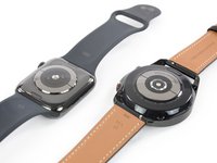
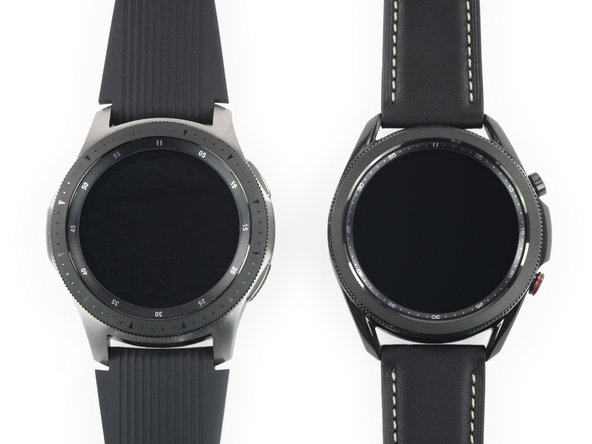
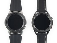
But let’s not compare apples to
orangesgalaxies. Here's an original Galaxy Watch (left) for a game of "spot the differences." -
The Watch3 has a smaller body, but a bigger screen (albeit at the same resolution). Also, its buttons are more classically watch-like.
-
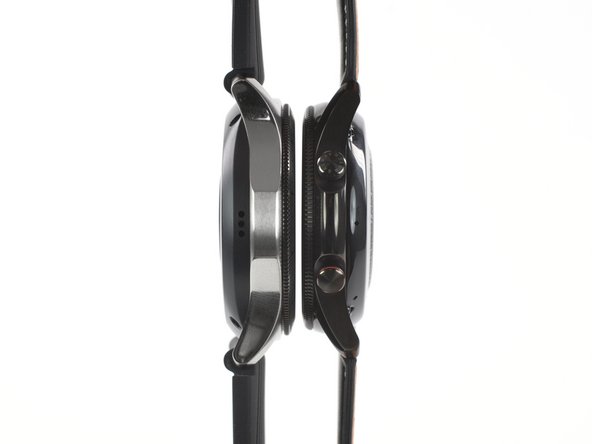
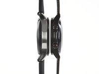
But it's what's inside that counts, right? The Watch3 now has eight optical sensors and ECG capabilities—but in this edge-on X-ray, the most recognizable bit to our eyes is the wireless charging coil.
-
There's a lot of layers in there, so let's start teasing it apart.
-
-
-
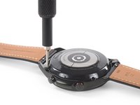
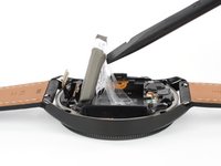
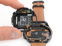
Opening the Watch3 is a familiar—and relatively painless—procedure, featuring tri-point screws and a rubber gasket.
-
While the back cover does feature a booby-trap sensor cable, its ample length makes it fairly benign. No traps were tripped in the making of this teardown.
-
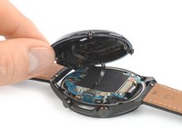
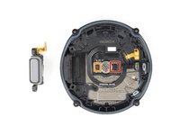
The ECG sensor, heart rate sensors, and wireless charging coil are all packed tightly into the monolithic back case—but not this freewheeling little speaker, with its nifty gasket.
-
The optical biosensing is handled by the Texas Instruments AFE49I30.
-
Texas Instruments TLV9002 1 MHz Operational Amplifier
-
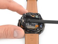
Modularity is neat! We approve. (Of the speaker, that is. We'll withhold approval of the other stuff until we find a way to extract it safely, which might take time.)
-
-
-
-
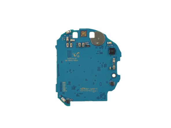
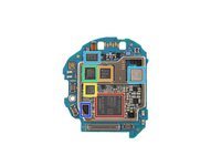
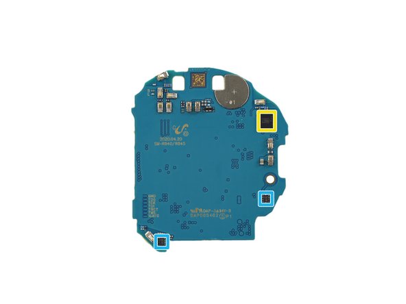
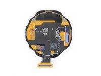
Scooping out this vaguely disc-shaped motherboard next, we peek under the shields and find:
-
A Samsung SiP FO-PLP combining the Exynos 9110 dual-core, 1.15 GHz Cortex-A53 processor, their in-house 1 GB DRAM and Power Management IC
-
Samsung Shannon 915 Intermediate Frequency IC
-
NXP PN80T NFC controller w/ Secure Element
-
Broadcom BCM430132 WiFi/Bluetooth module and Broadcom GNSS Location Hub for GPS/GLONASS/etc
-
Qualcomm Atheros QPA5580 Power Amplifier (likely)
-
IDT P9222S wireless power receiver
-
-
-
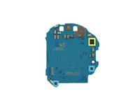
IC Identification, Pt. 2:
-
STMicroelectronics ST33G1M2 Secure Element
-
STMicroelectronics LPS22HB Pressure Sensor
-
STMicroelectronics LSM6DSOP 3-Axis Accelerometer and Gyroscope
-
Kinetic Technologies KTS1681 OVP Switch
-
Infineon BGSA14GN10 SP4T Antenna Tuning Switch
-
NXP Semiconductor BGU8309 GPS/GLONASS/Galileo/COMPASS low noise amplifier
-
-
-
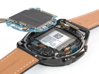
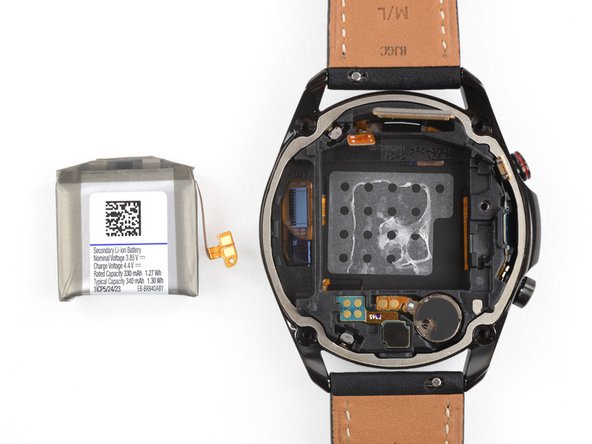
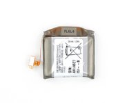
Only mild adhesive secures the battery pack, which we can dig out without using any heat. (Granted, the 90° F / 32° C weather here may have helped).
-
Our little friend is rated at a sober 1.3 Wh (340 mAh @ 3.85 V)—but with a claimed 2-day battery life, maybe Samsung just isn't concerned about winning the smartwatch battery spec war.
-
We half expected to find a novel battery design with a metal pouch—but so far, Apple seems to be the only watchmaker experimenting with that.
-
-
在这个步骤中使用的工具:Spudger$3.99
-
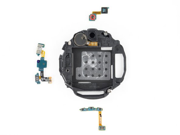
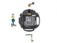
Our carbon fiber spudger is overkill for this midframe, which actually cooperates nicely as we lever it out. It reveals:
-
What might be a rubber-ensconced alti-barometric sensor
-
A modular cable combo with two
turntablesswitches and a microphone. -
Hall effect sensors that track the rotation of the outer bezel
-
And the vibration motor, slightly glued to the frame.
-
-
-
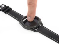
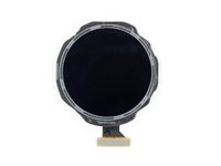
With the watch gutted, we finally have access to the circular AMOLED, always-on display. Except, well, it's not on right now. Obviously.
-
Although it was a journey getting here, the final step in this display removal only takes a single finger to pop it free from its frame.
-
Samsung was of course an early adopter of AMOLED tech in its mobile devices. But with Apple reportedly moving to microLED displays in the near future, it'll be interesting to see what happens next.
-
With that, it looks like we're out of time!
-
- The opening procedure is straightforward and glueless.
- No overlapping design of cables, no fragile ZIF connectors.
- The battery and display are easily accessible with some disassembly.
- An uncommon tri-point driver is needed for the back cover—regular Phillips on the inside.
- Most components are modular and can be replaced separately—except for the rear sensor array which is fixed to the back cover.
- The glass digitizer and screen are fused together—meaning glass-only repairs will be impractical.


最后的想法
可修复性评分


(10是最容易修复)

团队

Tobias Isakeit - Repairability Engineer Tobias Isakeit - Repairability Engineer 的会员
Business
1 名成员
创作了1,131篇指南
17条评论
Hi there. Wondering how easy it is to replace the glass on the back casing. Kits can be found online but haven't seen any pictures of it. Thanks.
I'm Curious. I wrote a comment in Januari and still no response regarding my question. Thanks for creating it, but where can put down a quest about it and get a respons.
Hi Erwin, this is a good place for your questions, another good place would be in the answers forum of the according device. Anyone who has an answer to your question can answer. Unfortunately I don’t know where exactly the eSIM chip is located, sorry. Usually those things are listed on the motherboard step of a teardown.