简介
是时候拆解史上“最大”的iPhone了——比去年的版本还要大一点点,iPhone 6s Plus配备了两种新技术。快点加入我们吧:
链接:iPhone 6s拆解|iPhone 6s|new_window=true
“拆解,欢迎回来!在iFixit,我们有一个习惯,那就是不放过任何机会,所以在第一部手机发布后,我们就把注意力集中在了大号手机上。”
还觉得不够吗?我们也觉得!请继续关注:
获取更多维修界的信息。
你所需要的
-
-
在我們把這個壞男孩放在小刀撬棒下之前,我們必須問:“嘿 Siri,引擎蓋下面是什麼?”:
-
帶有嵌入式 M9 運動協處理器的 Apple A9 處理器
-
16、64 或 128 GB 的存儲空間
-
5.5 英寸 1920 × 1080 像素 (401 ppi) 視網膜高清顯示屏,帶 3D Touch
-
12 MP iSight 攝像頭,支持 1.22µ 像素的 4K 視頻錄製,以及 5 MP FaceTime HD 攝像頭
-
7000 系列鋁製外殼和 Ion-X 玻璃
-
802.11a/b/g/n/ac Wi-Fi with MIMO + Bluetooth 4.2 + NFC + 23-band LTE
-
觸覺引擎
-
-
-
6s Plus 停下來拍攝特寫鏡頭,讓我們更好地了解定制的 7000 系列鋁合金 ,並標榜新型號:A1687
-
對這種新合金的早期分析 將其分解為約 91.17% 的鋁、0.08% 的鐵、7.64% 的鋅和 0.106% 的鎢。
-
較高的鋅含量應該會顯著提高 iPhone 6 中6063鋁合金 的抗拉強度(和製造成本)。
-
那個小''S'' 在新 iPhone 的大外殼上看起來格格不入——但是你還能用什麼方式向你的朋友展示你每年都會買一部新手機呢?
-
不過,蘋果公司鼓勵提早升級的新舉措對環境的打擊並不大。 正如 Apple 聲稱其設備可回收一樣,較短的產品壽命意味著二氧化碳排放量 增加和電子垃圾增多。
I would venture to say that most of the "old" iPhones get handed-down or sold second-hand. I have had EVERY iPhone since 2007 (yes, at some point every model... repairing/trading etc...) and I have sold or handed down every single one... I would imagine there are many more brands filing the waste basket when they have almost no resale value after the year is up...
Apple goes out of their way with planned obsolescence with every single one of their products, it isn't just phones. There is no reason why your $4,500 Mac book pro should not have an upgradable CPU, RAM, Storage, GPU, replaceable batteries, etc. Apple leads the pack when it comes to ripping you and mother nature off. PS, I'm no tree hugging hippie-crite... I'm using pure logic and common sense here. Yes, almost every maker of everything these days pushes planned obselessance. Apple is just the best at it. (Ever heard of the "Steve Jobs reality distortion field"? Well now it's just the apple reality distortion field now that his own arrogance and stupidity took him out of circulation. He was a horrible, I'm sorry to disrespect humanity this way, person, An extremely rich, yet morally worthless theif. Your argument is invalid sir.
-
-
-
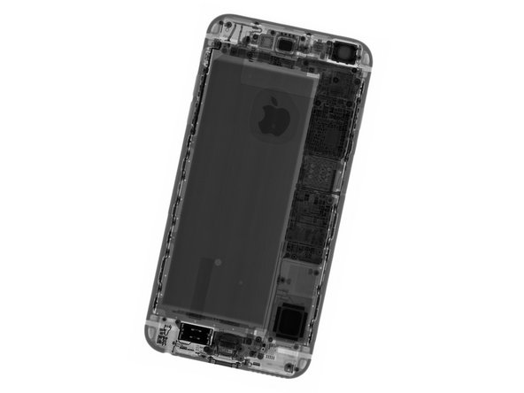
是時候先睹為快了! 像往常一樣,我們將用透視功能來爆破這款 iPhone:我們在 Creative Electron 的朋友將他們的 X 射線技術帶到了地下。
-
iPhone,你最好跑,你最好躲起來。
-
我們的工程師前往澳大利亞這片顛倒的土地為您帶來現場拆解,但如果沒有Macfixit 和 Circuitwise的盛情款待,我們無法做到這一點。
-
現在正是您一直在等待的時刻——讓我們開始拆解吧!
-
-
-
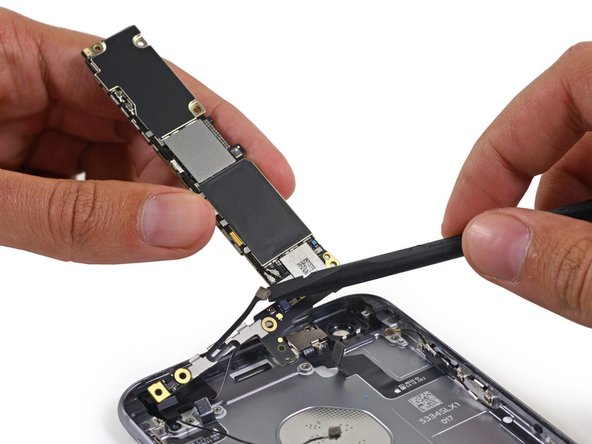
剛剛拆除了 6s,我們確切地知道從哪裡開始使用 Plus。
-
我們的拆解工程師只用了兩秒鐘就把手機拆開了——每顆螺絲一秒鐘,所有的小心都被拋在腦後。 (開個玩笑,他實際上非常小心並且從容不迫。這是我們僅有的 6s Plus。)
-
就像iPhone 6s拆解,6s Plus 的顯示屏組件周邊有一條膠帶。 對我們來說幸運的是,它沒有機會對抗反向钳。
-
隨著 Pentalobe 螺絲擰出和顯示屏粘合劑失效,我們開始了!
-
-
OK, I disassemble it, but there are screws with different length! Which one in which hole? Why didn’t you describe it? :(
This isn’t a guide. If it’s instructions you’re looking for, they’re located over here.
-
-
通過我們的撬棒輕彈三下,我們可以快速斷開並移除顯示屏組件。
-
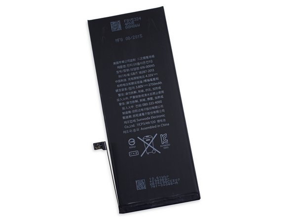
在我們繼續之前,我們把它放在秤上。 我們注意到 6s Plus 上的顯示屏組件重量為 80 克——而在去年的 6 Plus 上,它的重量僅為區區 60 克。
-
如此驚人的 33% 重量增加,全歸功於 Apple 全新的 3D Touch 技術。 那是一些沉重的東西。
-
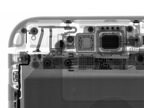
快速的 X 射線掃描顯示顯示器上有一些新的矽搭載——就像我們在 6s 上發現的那樣。
-
-
-
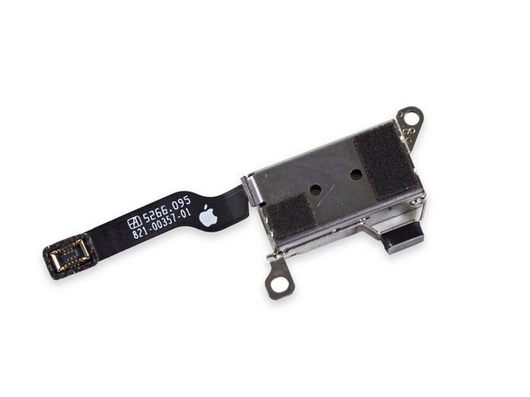
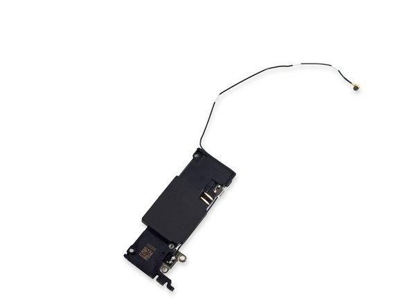
一個新支架固定(小!)Taptic Engine 及其新電纜。
-
6s Plus 中的 Taptic Engine 尺寸為 15 x 8 x 4.9 mm,而 6s 中的尺寸為 35 x 6 x 3.2 mm。
-
毫無疑問——它與所有組裝的東西都非常相配。
-
Taptic Engine 還有一個用於支撐麥克風的小橡膠緩衝器。
-
-
-
so iPhone 6S uses Apple A9 APL0898 SoC while iPhone 6S+ uses Apple A9 APL1022 SoC- does that mean those two are different products with different serial numbers?
APL numbers are associated with specific CPU dies within Apple Ax SoCs. These APL numbers are etched on CPU dies.
Apple SoC part number (SKU) is in form of 3xxSxxxx. Different CPU dies within same Apple Ax processor family result in different Apple SoC SKUs.
For example:
- APL0598 is CPU (part) number in Apple A6 SoC 339S0177 (in iPhone 5/5c)
- APL0698 is CPU (part) number in Apple A7 SoC 339S0207 (in iPhone 6s)
---- APL5698 is CPU (part) number in Apple A7 SoC 343S0665 (in iPad Air)
- APL1011 is CPU (part) number in Apple A8 SoC 339S00018 (in iPhone 6/6 Plus)
Thus, from not quite clear A9 SoC photo in iPhone 6S teardown:
- APL0898 is CPU (part) number in Apple A9 SoC 339S00114 (in iPhone 6S)
If APL1022 is marked on Apple A9 SoC SKU here (lack of SoC high resolution image does not allow me to see it) that should mean different processor die on iPhone 6S Plus as well as different A9 SoC SKU compared to A9 SoC in iPhone 6S.
I think you are also missing another Avago chip. You have AFEM-8030, but another site, www.teardowns.com with the teardown of the same Global LTE SKU, has two Avago chips:
1. AFEM8030 2. SFI530.
Are they wrong here?


32条评论
Shouldn't there be some differences in 14nm(Samsung, GloFo) and 16nm(TSMC) A9 chips (or am I wrong about TSMC technology)? Is it possible to track them?
Performance should be the same (same architecture and transistor count), but because of the smaller node used by Samsung, the A9 produced by them should a little cooler than the TSMC one.
Spotting which one is from TSMC or Samsung could be pretty difficult, since the temperature difference between chips could be less than 1-2 degrees.
Further investigation should be made with a X-ray microscope, the see the real differences between both manufacturers.
"In addition to the 70% faster CPU speed, it's also 90% faster for its GPU performance. The A9 also has the new M9 motion coprocessor that's built into the chip and is now always on."
apple.com
"A9 havs two 1.7GHz cores and two 1.2GHz cores."
forbes.com
Please call out the Invensense chip in the 6s plus. I'd imagine it is the same one as in the 6 phone but please confirm. Also, does Invensense have anything to do with the Optical Image Stabilization feature? Thanks.
Edvensense - 回复
I tried the taptic feedback 6S+ in a store and to be frank, it doesn't feel much different then using the old vibrate motors from any other phone. Granted, it does have faster reaction then those that use a spinning weight motor but looking at the old 6 Plus teardown, there really isn't that much of a difference. I mean seriously, go take a look and compare. The shape of the weights is a little different but the underlaying tech is basically the same. I don't see any reason why "3D touch" can't be incorporated on the old 6 Plus (other then to get people to buy the new phone). The hardware required for 3D touch (touchscreen + shaftless vibrator) is all available on the 6 Plus. The rest is simply software. Now you might say the 6S senses pressure but it really does not (please correct me with proof if I'm wrong). It doesn't have an actual pressure sensor like the macbooks. The screen (I believe) is using the size of your touch to determine pressure, not actual pressure.
As far as I know the 6S uses newly added capacitive sensors to measure the distance between display glass and backlight.
Thats why the 6S is a few grams heavier.
Look from Min 2:10 in the video "The Innovation behind 3D Touch":
Step 7: I think it's worh noting that while the 6S Plus's Taptic component is much shorter than the 6S's, it's volumetricly not much smaller. The 6S Plus's comes in at 588 mm³ while the 6S's is 672 mm³— just 14% larger.
Doing some back-of-the-enveloper math and shaving off 0.5 mm each dimension thats 478.5 mm³ for the 6S Plus and 512.325 mm³ for the 6S— 7% larger.
A teardown of the Taptic component could reveal that the internals in the 6S Plus's are the same size or even a hair larger. I'd like to see that teardown.
Where can i buy that fancy new ifixit screw driver? stop holding out!
jmcdonough - 回复
I'm wondering if the battery is the same dimensions as the 6 Plus because to be honest it seems like it does when I look at my 6 Plus without it's screen... If it is would it be possible to put a 6 Plus battery in the 6S Plus for the capacity?
Hynix E3NAND 16GB (128Gbit) partnumber should be H23QDG8UD1ACS not H230DG8UD1ACS (4th Letter is "Q" instead of "0"), but it's hard to read on the chip. BR Lars
i wonna iPhone 5
What is NB 30 mean for iPhone 6splus gold 128GB, it was written on repair service sheet. NB30?
I'm with you Lim, I haven't a clue what NB30 has to do with the iPhone 6s. However I do know that The NB in NB30 stands for NetBook. Chime in anyone
Does anyone know where the back microphone is located and is it replaceable.. Or do I need go change the main logic board in my iPhone 6S
@dfallen The rear mic is attached to the power button flex cable. You can find instructions for replacing it here.
There is a peice of rubber spacer/insulator fell off when I took the 6S plus apart. It looks exactly like the two used on the mounting ears for the Pentalobe screws that hold the iPhone together. However, I could not locate where this third piece of rubber spacer/insulator came from. Any idea?
William
my iphone keeps detecting that theres soemthing in the headphone jack but theres nothing connected. can i just like desolder the headphonejack out o the assemply and the iphone will think that its still there or will it detect that its missing and shut down until apple itself repairs it?
ya desarme pero no me acuerdo los tornillo en donde van ya que son de diferente tamaño