你所需要的
-
-
one phillips PH1 screw located on the back to remove the battery cover
-
-
-
Three Tri-point Y0 screws are located under the battery cover
-
Then the Red/White front plate comes out though the front
-
-
-
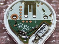
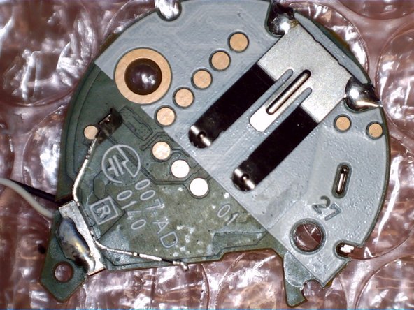
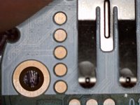
the PCB is set on three plastic supports with only the pressure of the back screws to lock it in place
-
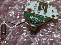
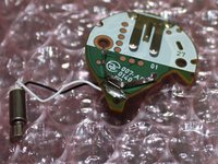
the PCB and vibration motor can be lifted out with only the slightest bit of pressure
-
-


18指南评论
This post needs moar wisdom
Anybody able to spot a Pedometer?
There is no pedometer. It's just a Bluetooth clicker. Your phone's sensors track all movement.
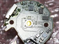
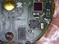
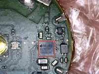
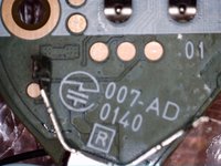
What is the
"A1
HNG
SBJ"
chip in "step 6"?
I2C/SPI flash?
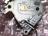
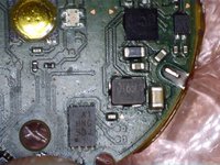
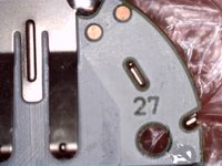
And.. what is in "Step 4" the chip? in between the capacitors and that "mostlikely MOSFETs for driving LEDs".
I'm looking at DA14580 modules on ebay:
http://www.ebay.com/sch/i.html?_from=R40...
And I tend to to say "let's try to clone this", the DA14580 has OTA programmable FLASH. :)
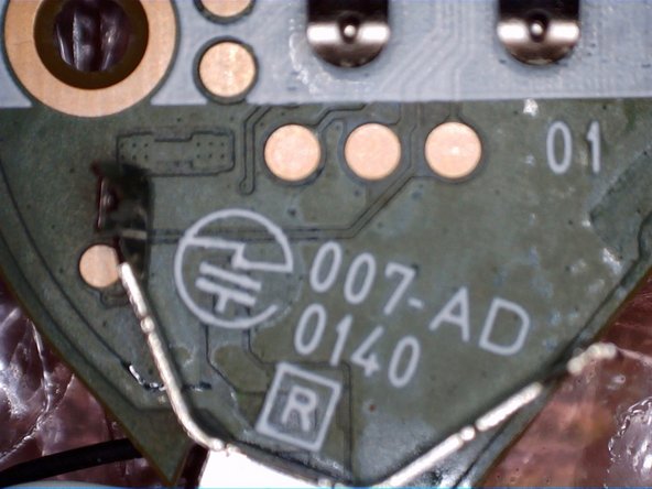
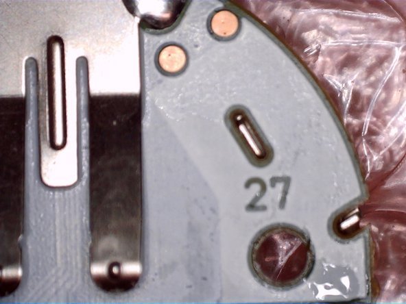
Last picture is most likely JTAG pogo contact points. For programming and testing. The board seems to be like 3-4+ layer board just based on the pictures. Also can't really tell you what chips those are with that quality of a picture. However the two little chips under the mounting hole on the picture in step 4 looks to be the DC Boost IC to keep constant voltage throughout the batteries life. The chip to the left of those boost converts is most likely the Bluetooth IC (just guessing by the location and the traces around it). Hope this helps :)
Jt Whissel - 回复