视频概述
-
-
这里有好多需要说的。让我们从硬件规格开始:
-
Nvidia Tegra X2 (Parker) SoC 配备两颗 Denver 2.0 64-bit 核心和四颗 ARM Cortex A57 64-bit 核心
-
集成了基于 Pascal 的 GPU 配备256个 CUDA 核心
-
8 GB RAM
-
128 GB 板载储存
-
Bluetooth 4.2,Wi-Fi 802.11ac/b/g/n,USB-C,3.5 mm 耳机接口
-
-
-
内容的生成始于Lightpack。它提供电力并处理信息,向头戴设备发送图像和声音数据。
-
同时, Lightwear 头戴设备会追踪控制器的位置和方向,并且测绘构建你周围环境的空间地图来帮助插入虚拟元素。
-
这些虚拟元素是如何生成的则完全是另外一个复杂的问题。
-
-
-
“混合现实”很复杂,但这和增强你在屏幕上看到的东西其实是一回事(就像智能手机或有外置摄像头反馈的 VR 显示设备)
-
更难的是增加显示,未经过滤的现实直接进入你的眼帘。要摆脱这种不实的错觉,Magic Leap One 使用了几种精巧的技术:
-
波导显示——本质上是一块透明的屏幕从侧面悄无声息的点亮。波导( Magic Leap 称之为“光子光场芯片”)引导光线——在这种情况下,一幅图像,穿过薄薄的一层玻璃,放大并投射入你的眼睛。
-
对焦平面 ——在 VR 显示设备上,一切都是同一焦距的。但在现实则不是这样——有些东西看起来很清晰但其他的看起来是模糊的,取决于你的眼睛的焦点在哪里。Magic Leap 通过合成多个波导来模仿这种现象——将图像分割为清晰的和模糊的区域。
-
-
-
让我们看看这东西都藏了什么光学的宝藏!一个快速测试排除了偏光片——我们必须要挖掘的更深一些来获得一些发现。
-
镜片的内部出人意料的丑陋,配备了频闪红外 LED ,一个有明显条纹的波导“显示”区域和一些奇怪的胶水使用。
-
波导由六个不那么漂亮的层压成,每层都有一个小的气隙。
-
边缘看起来像是手绘成的黑色,可能会最大限度地减少内部反射和干扰。
I would more tend to think that the waveguides are optically bonded and there are no air gaps. Usually optical bonding minimizes partial reflections at interfaces in order to increase overall contrast. But the waveguides must also rely on total internal reflection. That sounds like conflicting goals.
I was surprised by this as well, but I think if it were bonded all the way across with OCA you wouldn’t be able to see the obvious glue layers around the edges.
The waveguides work by total internal reflection (TIR) cause by the index of refraction mismatch between glass and air. If the layers of glass were bonded together with no gap (or other indexed mismatched material in between) then the light would exit the waveguide to the next layer an you don’t have a waveguide/TIR.
-
-
-
在头带的内侧,我们注意到有一个1级激光产品的标签。在你戴在眼睛前的设备上找到这个标签似乎是件很可怕的事情,但实际上在日常使用中是安全的,并不会比 CD 播放器更加危险。
-
旋开标准的梅花螺丝并移除了盖板,揭示了两个扬声器中的第一个是通过弹簧触点连接的,并通过色彩标记的垫圈保护着——到目前为止,可修复性很强。
-
同样隐藏在这块盖板下面的是:设备唯一的线缆的两个上端和一些帮助调整位置的磁力点。
-
但是从头带右侧突出的那个奇怪的黑色小盒子是什么?
-
-
The LED light ring is just for aesthetics, animations etc.
How do we know it’s AC or DC type magnetic tracking from this tear-down image?
28.5 kHz to 42.2 kHz https://www.tomshardware.com/news/magic-...
Source for the cube antennas https://neosid.de/en/news/3d-cube-antenn...
@tom0m Thanks for sharing! Cool find. Added a link in the teardown.
-
-
在拆下头戴和内面板之后,我们可以有更好的视角来观察眼部跟踪红外发射器。我们注意到它们都是串联连接,而不是单独控制。
-
终于,Magic Leap 的核心:光学和显示部件就在我们的指尖上了。
-
我们终于到这了,所以快系好安全带。
Could you please disassemble the strap as well? We haven`t seen a mechanism like this in any HMD yet. Packed in a small space, supposed to last years with enough force to keep it on various head sizes. I really want to know what kind of spring they used for this.
@tancho I only got a glimpse of it when we had it apart, but it looked like a single constant-force spring packed into the center plastic segment at the back.
-
-
-
-
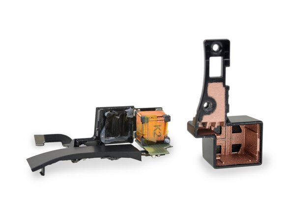
拆下其中的一个外部传感器阵列,我们在下面发现了一个光学系统用来将图像传进波导。
-
每个点工作在不同的深度——对应这单层的波导。
-
在背后,我们发现了世纪的显示设备:一个 OmniVision OP02222 场序彩色(FSC)LCOS 设备。这看起来是一个 OmniVision OP02222 的定制版本。
-
-
-
让我们更深入地了解光源和波导光学系统。
-
所以这六层都是干什么的?在两个不同的焦平面上有一个分离的波导来对应每个色彩通道(红绿蓝)。
-
如果没有特定于颜色的波导,每种颜色都会聚焦到稍有不同的点并使图像产生变形。
-
来自 Magic Leap 申请的 2016/0327789 专利的“Figure 6”对我们了解光学器件的内部如何工作有所启发。
-
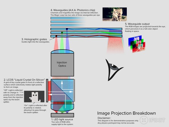
为了方便你的理解,我们自己为这个系统绘制了一幅“长到没法正常阅读的图像”,但是有猫。
The “tl;dr diagram” has the positions of the LED light source and LCOS grid swapped: Light from the LCOS will not be reflected into the waveguide. The figure from the Magic Leap patent is correct.
Jack Boyce - 回复
Well, yes and no. The position of the components shown in our diagram is correct—unlike in the patent drawing, the physical Leap One does have the light source at the back, firing forward (toward the waveguides). The LCOS grid is on the top, facing down. However, our graphic is incomplete and does not show every optical component—so if you’re trying to follow the light path through the entire system, you’re going to get tripped up and the system won’t “work.” Our graphic was originally meant to be a high-level conceptual overview and probably got too detailed for its own good. It certainly won’t satisfy any optics experts. But if you’re trying to understand the whole system, here’s a hint: there’s a mirror on the other side of the beam splitter, directly opposite the LCOS panel.
I wished there were more detailed images of complete breakdown of the projection system instead of trying explain the process. Some of us already have a good understanding of the process and have relied on IFIXIT to show us the components to verify our assumptions. With only few images we are still relying on vague block diagrams.
-
-
-
将所有的传感设备连接到头带上,我们得到了一个昂贵的分层柔性电缆:
-
Movidius MA2450 Myriad 2 视觉处理单元
-
SlimPort ANX7530 4K DisplayPort 接收器
-
OmniVision OV680 传感器桥用于同时处理多个相机的图像(就像我们在Amazon Fire 手机上找到的那个一样)
-
Altera/Intel 10M08V81G - 8000 逻辑单元 FPGA,可能用于胶合逻辑,或管理 MV 部件或摄像机桥数据
-
Parade Technologies 8713A 双向 USB 3.0 转接驱动器
-
NXP 半导体 TFA9891 音频放大器
-
德州仪器 TPS65912 电源管理芯片(PMIC)
This page is more useful to tell what’s inside the Altera/Intel 10M08V81G (the linked datasheet only lists operating conditions and specs that are of no interest to most people)
https://www.intel.com/content/www/us/en/...
Family table
The Myriad 2 is a vision processor, not a display processor. It’s going to be used here as a front-end processor for the cameras.
Fixed! Thanks for the tip. No idea how we managed to bungle that one—had a link to the right datasheet but somehow not the description. :p
“Possible camera combiner chip” is more specifically the OmniVision OV00680-B64G Sensor Bridge
Good find—thanks for sharing! We’ve updated the description.
With the way TI marks packages, “78CS9SI” is not the part number; use the second number instead. It’s tough to tell exactly from the image, but it looks like it might be “65912,” which would make it the TPS65912 power management unit chip.
Confirmed (again—2 for 2!). Thanks a ton!
-
-
-
现在事情变得有点破坏性了,但是为了看看光学链是值得的。
-
一个有六个 LED 的小圆环开始这次操作,分别是红绿蓝,为了两个焦平面配备了两套。
-
然后 LED 在 LCOS 微显示器上发光以产生图像,它安装在隔壁的黑色塑料外壳上。
-
从该外壳的内部,准直透镜对准来自 LED 的原始光输出,而且它安装在一个偏振分束器上。
-
然后,偏振光束通过一系列透镜,将图像聚焦到波导上的入射光栅上。
-
入射光栅本身看起来像嵌入六个波导中(现在略微破碎的)小点。
-
我们拿起“投影”单元进行仔细观察,发现了与每个入口光栅相关的颜色:两个红色,两个绿色和两个蓝色。
Thanks for this. It also explains the process they are using to derive the six planes, which incidentally corresponds to the six color fields the OmniVision LCOS is capable of generating at I assume 1/360th of second per field. However this does not explain how they can sustain a two complete RGB frames in 1/60th of second unless the image resolution is 1280x720 (allowing 120 fps) instead of 1920x1080 (60 fps). Unless they multiplex the six LEDs at 1/360th of second with two frames of image information. Essentially if the resolution is 1080P (unlikely) the NVIDIA TX2 is processing two (1920 x 2) x 1080 images (one for each eye) every 1/60th of second. Pretty impressive, but I think it is actually just 720P as confirmed in my Unity SDK the image is 1280 x 960.
-
-
-
我们已经享受完光学大餐,是时候把我们的注意力转向这个装置的大脑—— Lightpack!
-
很难不去注意到这个突出的超酷通风口。这太小小的口袋 PC 有没有一个强劲的散热系统?我们马上就能知道。
-
这个 FCC 标记没有放弃自己,其他的就是——由 Magic Leap 设计,在墨西哥组装。事实上的硬件制造厂商的身份据说是一个被严格保密的秘密。
-
-
-
在拆开了几个外壳之后,是时候看看让这魔法发生的芯片们了:
-
两个 Samsung K3RG5G50MM-FGCJ 32 Gb LPDDR4 DRAM(共 64 Gb 或 8 GB )
-
Murata 1KL (像是 Wi-Fi/Bluetooth 模块)
-
Nordic 半导体 N52832 RF SoC
-
Renesas Electronics 9237HRZ 降压 - 升压电池充电器
-
Altera(英特尔拥有)10M08 MAX 10 现场可编程门阵列
-
Maxim Semiconductor MAX77620M 电源管理IC 和 Parade Technologies 8713A双向 USB 3.0转接驱动器
Yellow box is not Parade Technologies 8713A , that is WIFI AC, BT MODULE from Murrata
Thanks for pointing that out, I’d mixed up two chips. It’s correct now.
-
-
-
背后还有更多的魔法:
-
东芝 THGAF4T0N8LBAIR 128 GB NAND 通用闪存
-
Spansion (现为 Cypress) FS128S 128 Mb 四路 SPI NOR 闪存
-
德州仪器 TPS65982 USB Type-C 和 USB 供电控制器
-
uPI 半导体 uP1666Q 2相降压控制器
-
德州仪器 INA3221 双向电压监视器
-
-
Palmer got fired for lying and stealing. He broke signed contracts and without community involvement or their consideration is now a mod at Reddit in violation of several moddiqette rules. He is a joke and you disgrace yourself accepting anything from him.


15条评论
In Step 10, figure 2 (the figure from the patent) the ‘optional’ polarizing filter (2072) is not very optional. And you skipped it in your summary image.
It’s likely a three-wavelength, 1/4-wave retarder used to rotate linearly-polarized light to circularly-polarized light before it bounces off the LCOS. The reflected light goes through another 1/4 wave so it’s now 1/2 a wave from the input light. That is - it’s linearly polarized 90 degrees from the original light. That’s why the polarizing beam splitter cube is able to separate the input field (100% coverage) from the LCOS-reflected fields. They’re 90 deg. different polarization.
Also, that means the RGB emitters aren’t likely LED’s. They’d have to be laser diodes (or VCSEL’s) to have the narrow spectrum necessary for the 1/4 wave retarding film.
Wick, you seem to know something about this subject, but you are wrong about the Figure from the patent. The beam splitter will polarize the light but having two might work better.
In the final configuration and as diagrams by iFixit (the 3rd figure with respect to Step 10) they absolutely need a polarizer (as show) right after the LEDs or else half the light will go strait into the injection optics without modulation. This 3rd figure does leave out a quarter-wave plate and polarizing mirror on the right side of the beam splitter cube that is necessary to bounce the light back to the beam splitter so it can be directed out to the injection logic. As drawn, the light from the LCOS would go through the beam splitter and out the side of the cube.
I want to add to my prior comment that I have only seen the teardown pictures and had to mentally reconstruct what was going on from picture. I did not see the components as they were taken off. Based off the pictures, I was trying to make it work based on what I was seen from static pictures.
Something that concerns me in this design is that the LED light is shot straight at the beam splitter and if the polarization is not great with the first/LED polarizer and the beam splitter, there will be a spot of uncontrolled light (about the size of the LEDs) in the center of the image. I’m assuming they are using wire grid polarizers in both locations.
Another issue with the design is that the image has to pass through and reflect off the beam splitter (if based on what I was shown and was told is correct). Usually with a wire grid polarizer, you don’t want to pass the “image” of the LCOS through the polarizer as it will do damage to the image. The FIG 6 from the patents would be the “normal” configuration.
Ye-gods, thats a lot of impressive technology squeezed into a small package! No wonder it has taken so long to develop. I’m skeptical that it will ever be a commercially viable product. They are surely shipping significant dollars along with each developer unit. My prediction is that, at best, it will be a high-end business-use product, never a consumer product. Most probably MagicLeap will be acquired by a major before too long, and a year later the major will kill it, having found the skeletons in the closet and determined it will never be profitable — especially with consumers now embracing lower-tech, lower AR quality devices. But hey, congrats to ML for being aggressive with technology, and I wish them the best of luck. Thanks for the superb tear-down, finally revealing the long-standing mystery of ML, IFIXIT!
lannierose - 回复
The device is reminiscent of a camcorder, with a lot of optics and electronics compressed into a small volume and not a lot of consideration to repairability. There’s a lot more engineering here than a VR headset and I’m impressed how far Magic Leap has iterated the design for a developer release. That said, having a non-replaceable battery would be a disaster for a consumer release IMHO. Great teardown!
Jack Boyce - 回复
Every bit of the teardown proves my thought that ML was in full “use whatever it takes to get something awesome and tangible into the light of day and hands of tech journalists”.
The idea of ML’s defining headlines being stuff that had words like “failure, $500M+, defunct, etc” was something they were going to break everything to avoid.
This iteration of the tech is a proof of concept device purely for the sake of quieting naysayers and settling the growing number of very worried investors and future buyers.
If this operates at even 75% “WOW Factor” it may earn them the time they need to finish designing their actual consumer level device. I have a feeling their mass production model will barely resemble this. The battery placement and total absense of maintenance/repair/replace indicators kinda proves that.
I am skeptical that the mass-produced model will ever be a reality, but I have a bit more hope than normal now that I've seen the Nissan GTR level of obsessive care in the build quality of this device.
Also, I didn't have enough space to write how absolutely blown away I am at the quality of this teardown. Beyond just the physical work, the extra research put into explaining it is brilliant. The confusing bits of tech are easy to understand and including the links tobsources and part data right with the test instead of just a pile of footnotes at the bottom helps let me decide just how deep down the tech rabbit hole I want to go!
I've read and loved many of these from ifixit, but you guys/girls/robots have reset the bar (again) with this one. Well done!
I agree, this is absolutely awesome work by ifixit!
Confused with one camera can magic leap track each eye independently?
One eye-tracking camera per eye, you can see the corresponding black square in the lens opposite the one we opened up!
Has iFixit torn down the Microsoft HoloLens from 3 years ago?
How does Magic Leap One compare to the HoloLens??
@johnwnguyen We have not. My understanding is HoloLens uses a waveguide display as well, albeit with a narrower field of view. Magic Leap One also has the benefit of an additional focus plane, although how much that actually contributes to the experience I couldn’t say. If you want the details, I can’t recommend Karl’s blog highly enough—he sniffed out Magic Leap’s trail early and correctly predicted that they’d use display technology more similar to HoloLens than not. (He’s a bit hard on Magic Leap at times, but IMO does a great job cutting through the hype and presenting all the known facts.) Palmer’s writeup also makes numerous comparisons to the HoloLens, summing up Magic Leap One as “slightly better than Hololens in some ways, slightly worse in others, and generally a small step past what was state of the art three years ago – this is more Hololens 1.1 than Consumer AR 1.0.” Worth a read.
I’m curious about the microphones, I’ve seen that there may be four of them. Are these in the “sensor arrays”? Where are they aimed? Are they being processed by a chip and then input into the processor, or are they all processed in realtime by the processor unit?
Comentar que ya he tenido varias Magic Leap One Creator Edition, Size 1 y Size 2, y todas al cabo de unos meses se han roto, en concreto el problema es que al abrir y cerrar la diadema para colocar en la cabeza, el pequeño conector y cable flex que conecta el sensor magnético se rompe y deja inutilizable las gafas por completo, sin el mando controlador no se pueden usar. Un fallo terrible de diseño al estilo flexgate de los macbook pro. // Comment that I have already had several Magic Leap One Creator Edition, Size 1 and Size 2, and all of them have broken after a few months, specifically the problem is that when opening and closing the headband to place it on the head, the small connector and the flex cable that connects the magnetic sensor breaks and makes the glasses completely unusable, without the controller they cannot be used. A terrible design flaw in the flexgate style of the macbook pro.
The CUDA cores are a fixed feature of the Parker SoC - not a separate semiconductor. They don’t deserve an individual bullet in this listing.
alexander.stohr - 回复